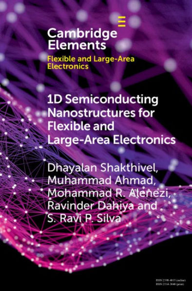
1D Semiconducting Nanostructures for Flexible and Large-Area Electronics: Growth Mechanisms and Suitability

1D Semiconducting Nanostructures for Flexible and Large-Area Electronics: Growth Mechanisms and Suitability

1D Semiconducting Nanostructures for Flexible and Large-Area Electronics: Growth Mechanisms and Suitability

1D Semiconducting Nanostructures for Flexible and Large-Area Electronics: Growth Mechanisms and Suitability

eBook

$18.99  $25.00 Save 24% Current price is $18.99, Original price is $25. You Save 24%.

Available on Compatible NOOK devices, the free NOOK App and in My Digital Library.
WANT A NOOK?  Explore Now

Related collections and offers

LEND ME® See Details

Overview

Semiconducting nanostructures such as nanowires (NWs) have been used as building blocks for various types of sensors, energy storage and generation devices, electronic devices and for new manufacturing methods involving printed NWs. The response of these sensing/energy/electronic components and the new fabrication methods depends very much on the quality of NWs and for this reason it is important to understand the growth mechanism of 1D semiconducting nanostructures. This is also important to understand the compatibility of NW growth steps and tools used in the process with these unconventional substrates such as plastic that are used in flexible and large area electronics. Therefore, this Element presents at length discussion about the growth mechanisms, growth conditions and the tools used for the synthesis of NWs. Although NWs from Si, ZnO and carbon nanotubes (CNTs) are included, the discussion is generic and relevant to several other types of NWs as well as heterostructures.

Product Details

ISBN-13: 9781108624169
Publisher: Cambridge University Press
Publication date: 10/31/2019
Series: Elements in Flexible and Large-Area Electronics
Sold by: Barnes & Noble
Format: eBook
File size: 17 MB
Note: This product may take a few minutes to download.

Table of Contents

1. Introduction; 2. VLS growth mechanism for Si NWs; 3. Carbon nanotubes; 4. ZnO nanomaterials; 5. Suitability of inorganic NWs for large area flexible electronics; 6. Summary and conclusions.
From the B&N Reads Blog

Customer Reviews