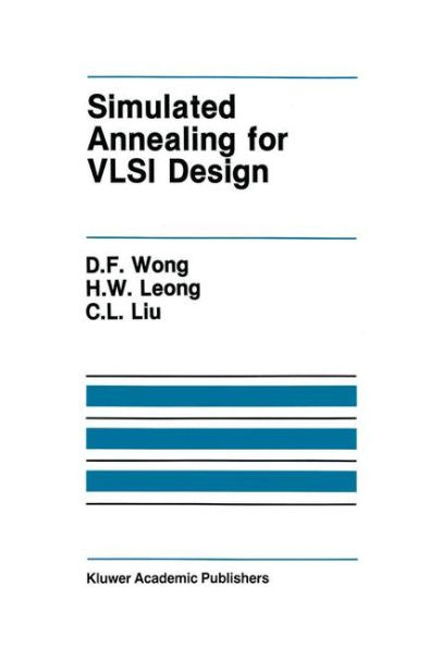
Simulated Annealing for VLSI Design / Edition 1

Simulated Annealing for VLSI Design / Edition 1

ISBN-10:
0898382564
ISBN-13:
9780898382563
Pub. Date:
03/31/1988
Publisher:
Springer US
ISBN-10:
0898382564
ISBN-13:
9780898382563
Pub. Date:
03/31/1988
Publisher:
Springer US
Simulated Annealing for VLSI Design / Edition 1

Simulated Annealing for VLSI Design / Edition 1

Hardcover

$109.99
Current price is , Original price is $109.99. You
$109.99 
  • SHIP THIS ITEM
    Qualifies for Free Shipping
  • PICK UP IN STORE
    Check Availability at Nearby Stores

Overview

This monograph represents a summary of our work in the last two years in applying the method of simulated annealing to the solution of problems that arise in the physical design of VLSI circuits. Our study is experimental in nature, in that we are concerned with issues such as solution representations, neighborhood structures, cost functions, approximation schemes, and so on, in order to obtain good design results in a reasonable amount of com­ putation time. We hope that our experiences with the techniques we employed, some of which indeed bear certain similarities for different problems, could be useful as hints and guides for other researchers in applying the method to the solution of other problems. Work reported in this monograph was partially supported by the National Science Foundation under grant MIP 87-03273, by the Semiconductor Research Corporation under contract 87-DP- 109, by a grant from the General Electric Company, and by a grant from the Sandia Laboratories.

Product Details

ISBN-13: 9780898382563
Publisher: Springer US
Publication date: 03/31/1988
Series: The Springer International Series in Engineering and Computer Science , #42
Edition description: 1988
Pages: 202
Product dimensions: 6.14(w) x 9.21(h) x 0.24(d)

Table of Contents

1. Introduction.- 1.1. Combinatorial Optimization.- 1.2. The Method of Simulated Annealing.- 1.3. Remarks.- 2. Placement.- 2.1. Introduction.- 2.2. Gate-Array Placement.- 2.3. Standard-Cell Placement.- 2.4. Macro/Custom-Cell Placement.- 2.5. Other Shastic Algorithms.- 2.6. Concluding Remarks.- 3. Floorplan Design.- 3.1. Introduction.- 3.2. Part 1: Rectangular Modules.- 3.3. Part 2: Rectangular and L-Shaped Modules.- 3.4. Concluding Remarks.- 4. Channel Routing.- 4.1. Introduction.- 4.2. The Channel Routing Problem.- 4.3. The Channel Router SACR.- 4.4. The Channel Router SACR2.- 4.5. Experimental Results and Discussion.- 4.6. Concluding Remarks.- 5. Permutation Channel Routing.- 5.1. Introduction.- 5.2. Motivation and Applications.- 5.3. NP-Completeness Results.- 5.4. First Method — Simulated Annealing.- 5.5. Second Method — Iterative Improvement.- 5.6. Experimental Results.- 5.7. Concluding Remarks.- 6. PLA Folding.- 6.1. Introduction.- 6.2. The PLA Folding Problem.- 6.3. The PLA Folding Algorithm.- 6.4. Multiple-Folded PLA Realization.- 6.5. Constrained Multiple Folding.- 6.6. Simple Folding.- 6.7. Experimental Results and Discussions.- 6.8. Concluding Remarks.- 7. Gate Matrix Layout.- 7.1. Introduction.- 7.2. Problem Formulation.- 7.3. Generalized Problem Formulation.- 7.4. Advantages of the Generalized Formulation.- 7.5. The Simulated Annealing Method.- 7.6. Experimental Results.- 7.7. Concluding Remarks.- 8. Array Optimization.- 8.1. Introduction.- 8.2. The Array Optimization Problem.- 8.3. Definitions.- 8.4. The Array Optimization Algorithm.- 8.5. Experimental Results.- 8.6. Concluding Remarks.- References.
From the B&N Reads Blog

Customer Reviews